
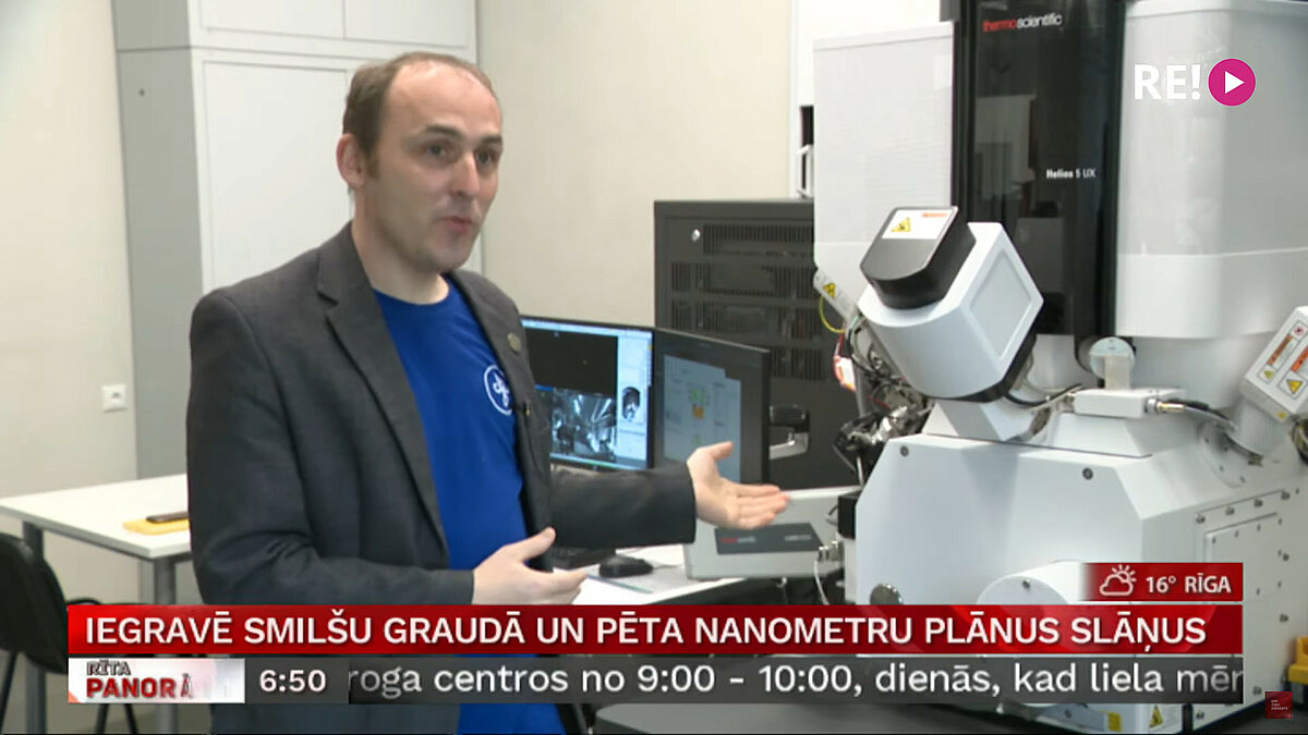
On June 9, on the National TV morning news program “Rīta Panorāma”, ISSP UL’s scientist Krišjānis Šmits, who heads the Laboratory of Materials Morphology and Structure Investigation, explained that the scanning electron microscope can work with things as tiny as a nanometer or one-billionth part of a meter. This device Helio 5 UX is also an ion microscope and it is the best in Latvia and in the Baltic Sea countries.
The scientist also explained that with scanning electron microscope it is possible not only to look at really tiny things, but also to engrave several letters, for example, in a grain of sand. However, the microscope at the laboratory is used to check the thickness of the transistor layers to be inserted in mobile phone processors, which are usually about seven nanometers thin. With the help of a scanning electron microscope, it is also possible to investigate multilayered glasses, OLED lamps, antibacterial coatings, and many other new materials.